Samsung starts production of 290-layer V-NAND chips
이 글자크기로 변경됩니다.
(예시) 가장 빠른 뉴스가 있고 다양한 정보, 쌍방향 소통이 숨쉬는 다음뉴스를 만나보세요. 다음뉴스는 국내외 주요이슈와 실시간 속보, 문화생활 및 다양한 분야의 뉴스를 입체적으로 전달하고 있습니다.
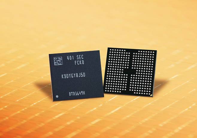
Samsung Electronics, the world’s largest memory chip maker, said Tuesday it kicked off the mass production of its one-terabit triple-level cell vertical NAND, or V-NAND, which is about 50 percent denser and 10 percent more energy efficient than its predecessor that launched in 2022.
“We are excited to deliver the industry’s first 9th-gen V-NAND which will take future applications leaps forward. To address the evolving needs for NAND flash solutions, Samsung has pushed the boundaries in cell architecture and operational scheme for our next-generation product,” said Hur Sung-hoi, head of flash product and technology at Samsung Electronics.
Through the latest V-NAND mass production, the company looks to set the trend for the high-performance, high-density solid-state drive market that meets the needs of the coming artificial intelligence generation, Hur added.
Samsung did not disclose the specifics, but industry sources say the firm has started mass production of its 9th-generation 290-layer V-NAND products with the industry's smallest cell size and thinnest mold.
To enhance the new product’s quality and reliability, Samsung applied innovations such as cell interference avoidance and cell life extension, while eliminating dummy channel holes has significantly reduced the planar area of the memory cells.
Samsung’s advanced “channel hole etching” technology realizes electron pathways by stacking mold layers and maximizes fabrication productivity as it enables simultaneous drilling of the industry’s highest cell layer count in a double-stack structure.
As the number of cell layers increases, the ability to pierce through higher cell numbers becomes essential, demanding more sophisticated etching techniques, according to Samsung.
Samsung said the latest V-NAND is equipped with the next-generation NAND flash interface -- Toggle 5.1 -- which supports increased data input and output speeds by 33 percent to up to 3.2 gigabits-per-second.
It also has advanced low-power design for power consumption improvement as customers’ needs for reducing energy usage and carbon emissions became vital.
On the same day, the memory chip maker also unveiled its plan to accelerate its efforts on the development of high-capacity and high-performance NAND required in the AI era. The mass production of the quad-level cell model for the ninth-generation V-NAND is set to begin in the second half, the company said.
During a third-quarter earnings conference call in October last year, Samsung announced that it aims to develop 1,000-layer NAND chips by 2030 for higher density and storage capabilities to gain ground in the fast-growing NAND flash market, in line with rapidly expanding AI technologies.
According to market research firm Omdia, NAND flash sales globally are expected to grow at an average annual growth rate of 24 percent from $38.7 billion in 2023 to $114.8 billion by 2028.
By Jie Ye-eun(yeeun@heraldcorp.com)
Copyright © 코리아헤럴드. 무단전재 및 재배포 금지.