Samsung Elec to employ 1.4 nano process in foundry output by 2027
![Choi Si-young. [Photo by Samsung Electronics Co.]](https://img4.daumcdn.net/thumb/R658x0.q70/?fname=https://t1.daumcdn.net/news/202210/04/mk/20221004112705826gnqe.jpg)
Samsung Electronics during an annual Samsung Foundry Forum event held on Sunday (local time) in San Jose, California, announced that it will adopt 2nm process technology by 2025 and mass produce on 1.4nm process technology by 2027 to triple production capacity by 2027.
“The technology development goal down to 1.4nm and foundry platforms specialized for each application, together with stable supply through consistent investment are all part of Samsung’s strategies to secure customers’ trust and support their success,” said Dr. Choi Si-young, president and head of Foundry Business at Samsung Electronics. “Realizing every customer’s innovations with our partners has been at the core of our foundry service.”
The Korean chip giant unveiled a plan to begin mass production on 1.4nm process technology earlier through advanced packaging and process technology. Samsung in 2015 mass produced FinFET transistors and in June this year began enhancing its gate-all-around (GAA)-based 3nm process technology to win clients in high-performance and low-power semiconductor markets such as HPC, automotive, 5G and the Internet of Things (IoT).
TSMC earlier announced shift to 1.4nm technology, but it is yet to detail the roadmap.
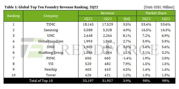
The global market share of Samsung Electronics’ foundry sales reached 16.5 percent in the second quarter this year, up 0.2 percentage point from 16.3 percent during the first quarter while the top foundry company TSMC’s dropped by 0.2 percentage point to 53.4 percent over the same period.
The Korean chip giant is forecast to invest $192.1 billion in total to build 11 semiconductor plants in Texas to expand its foundry market share.
During the forum, Samsung Electronics also announced a plan to speed up the development of 2.5D/3D heterogeneous integration packaging technology, which integrates separately manufactured chips into a higher-level assembly.
Samsung is planning to continue innovating I-Cube which incorporates four High Bandwidth Memories (HBMs) and one logic die as well as eXtended-Cube (X-Cube), which allows chip-stacking of SRAM dies on top of a base logic die. The company plans to ready mass production of 3D packaging X-Cube with micro-bump interconnection for mass production in 2024, and the bump-less X-Cube will be available in 2026.
Samsung is also expanding its production capacity by more than three times through its “Shell-First” strategy where it begins production even before receiving orders.
Shares of Samsung Electronics traded up 3.77 percent at 55,100 won ($38.42) during Tuesday morning trade.
[ㄏ Maeil Business Newspaper & mk.co.kr, All rights reserved]
Copyright © 매일경제 & mk.co.kr. 무단 전재, 재배포 및 AI학습 이용 금지
- Seoul may employ pandemic emergency stock relief of $7 bn fund and short sale ban - Pulse by Maeil Business News Korea
- Korea’s battery trio would likely deliver better-than-expected Q3 earnings - Pulse by Maeil Business News Korea
- Korean banks’ net debt offering hit record high in Sept to fan market yields - Pulse by Maeil Business News Korea
- KB Kookmin Bank readies another rescue fund for Indonesian unit KB Bukopin - Pulse by Maeil Business News Korea
- Toolgen gains upper hand in CRISPR patent dispute over US schools - Pulse by Maeil Business News Korea
- 강경준, 상간남 피소…사랑꾼 이미지 타격 [MK픽] - 스타투데이
- AI가 실시간으로 가격도 바꾼다…아마존·우버 성공 뒤엔 ‘다이내믹 프라이싱’- 매경ECONOMY
- 서예지, 12월 29일 데뷔 11년 만에 첫 단독 팬미팅 개최 [공식] - MK스포츠
- 이찬원, 이태원 참사에 "노래 못해요" 했다가 봉변 당했다 - 스타투데이
- 양희은·양희경 자매, 오늘(4일) 모친상 - 스타투데이